Group Nguyen Krajewski others
Group members
- Khai Nguyen
- Hoang Bach Nguyen
- Ly Thai Hoa
- Miglio Krajewski
1. PCB Milling Equipment and Tooling
Tool Types
The PCB milling machine uses several types of milling and drilling tools depending on the machining step.
| Tool Type | Size | Purpose |
|---|---|---|
| Universal Cutter | 0.2 mm | Trace isolation milling |
| End Mill | 1 mm | Pocket milling and routing |
| Spiral Drill | 2 mm | Drilling holes |
| Contour Router | 2 mm | Cutting PCB outline |
These bits are used to engrave and separate copper traces on PCB boards during CNC milling.
Typical usage examples
- 0.1-0.2 mm V-bit : very fine trace milling
- 0.8-1 mm end mill : clearing wider areas
- 1-2 mm contour routers : enlarge drilled holes and cut edges
2. PCB Milling Machine Setup
Starting the System
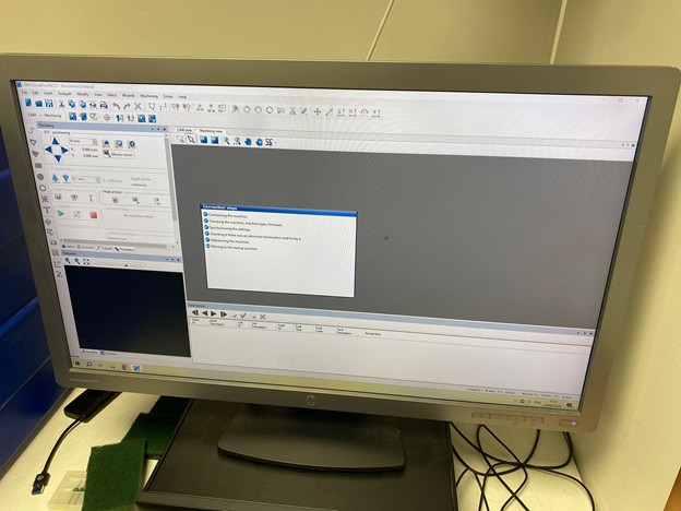
Turn on the computer
- Turn on the computer and open the PCB milling software, check if there is no error
Turn on the milling machine
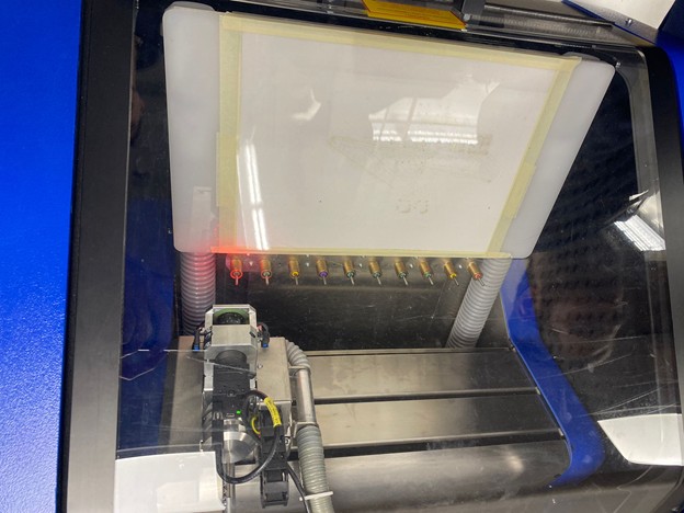
- Turn on the PCB milling machine using the switch on the side of the table, A red indicator light confirms the machine is powered.
PCB milling bits
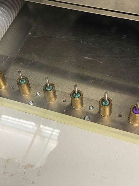
PCB milling bits used for engraving printed circuit boards on CNC machines.
They are used for: Trace milling, separating copper traces on the PCB. Outline cutting, cutting the board from the FR-1 sheet. Each bit has a different diameter and angle:
Bit Types
- 0.1–0.2 mm V-bit for very small trace milling
- 0.8–1 mm endmill for drilling or cutting outlines
- 1-2 mm contour routers for enlarge drilled holes and cut edges
3. Importing and Preparing PCB Design
Using the Process Planning Wizard, the PCB design file (Gerber format) is imported into the CAM software.
The software automatically:
- Analyzes PCB layers
- Determines machining steps
- Assigns tools
- Generates CNC toolpaths
Process Planning Wizard
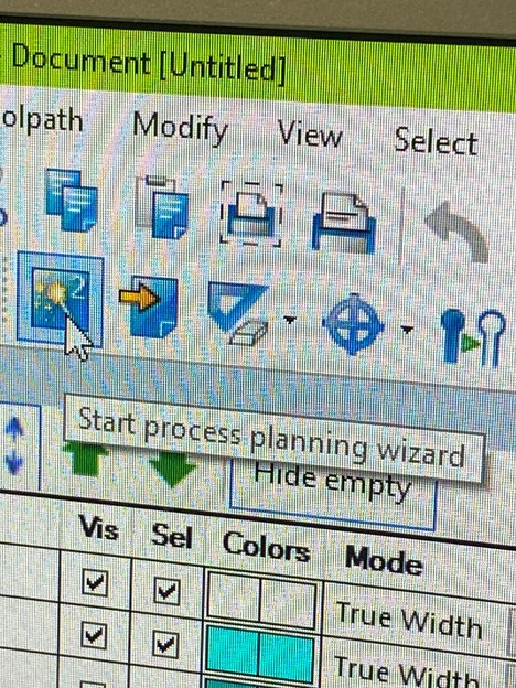
- Click "Start process planning wizard"
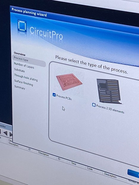
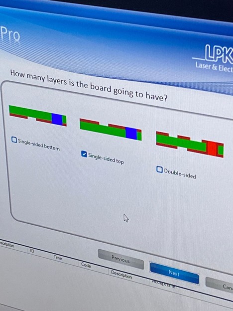
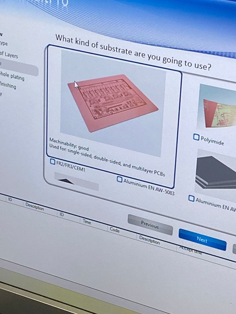
Type of Process, Board Layers, and Type of Substrate
-
Process type: PCB process
-
Board type: Single-sided top
-
Substrate material: FR4 or FR5
4. Gerber file check
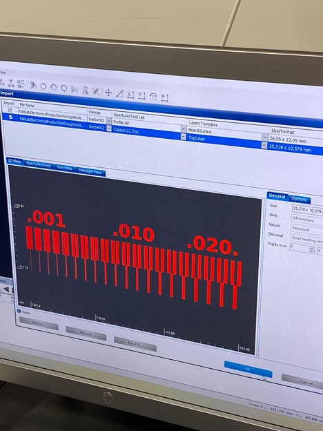
The file we selected was a PCB test pattern design. Check the design before going to the machining step.
The PCB test design contains traces of varying width to evaluate manufacturing limits.
| Width (inch) | Width (mm) | Purpose |
|---|---|---|
| 0.001 | ~0.025 mm | Ultra‑fine test trace |
| 0.010 | ~0.254 mm | Standard trace |
| 0.020 | ~0.508 mm | Large trace |
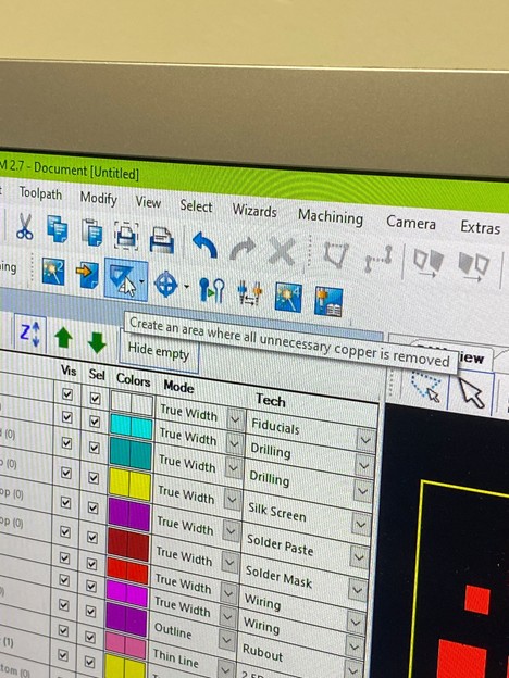
Extra buttons that will be important
Unnecessary copper area
This button makes an area where all unnecessary copper is removed.
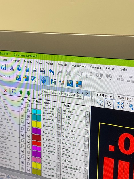
Fiducials
This one is for create positioning feducials (reference points) on the PCB. They are used to:
- determine the precise position of the PCB
- help the machine align its coordinates
- ensure drilling and milling are in the correct position
5. Isolation Milling Setup
Generate isolation and contour routing toolpath is used to automatically generate toolpaths for CNC PCB milling.
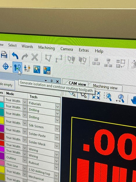
After clicking, you will see the Technology Dialog, which displays the information:
- Material type: FR4 (PCB material type)
- Copper layer thickness: 18 µm
- Isolation method: Basic
This means the software is preparing how the machine will mill to separate the copper traces.
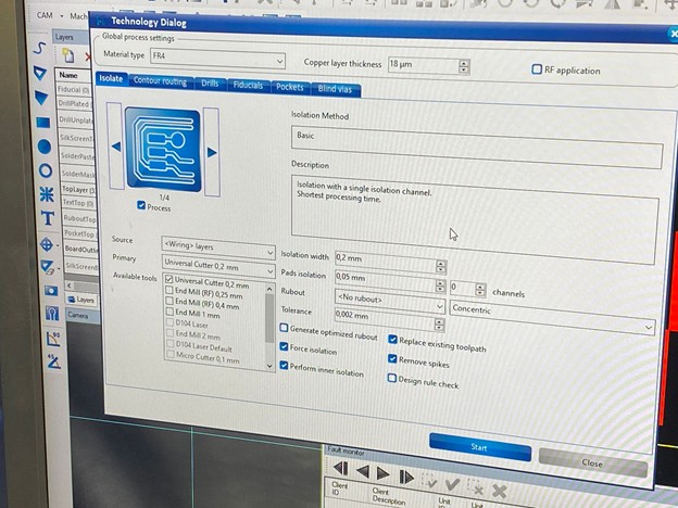
Important parameters are being set
Isolation width = 0.2mm
This means the machine will mill a 0.2 mm wide groove to separate the traces.
Tool (milling cutter)
The list of tools is on the left:
- Universal Cutter
- End Mill
- Micro Cutter
- The software will select the appropriate milling cutter to create the isolation.
Pad Isolation = 0.05 mm
The distance between the component pad and the surrounding copper.
6. Contour and Pocket routing
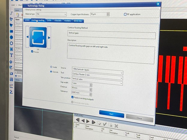
Contour Routing Settings
-
Routing Method: Vertical gaps — small tabs are left so the PCB stays attached to the FR4 board during cutting.
-
Tool: 2 mm contour router — used to cut the PCB outline.
-
Gap Width: 1 mm — width of the holding tabs.
-
Gap Distance: 50 mm — spacing between the tabs.
-
Cut Direction: Outside — the machine cuts outside the PCB outline to keep the correct board size.
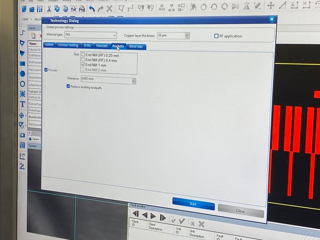
Pocket Routing Settings
Pocket milling removes larger copper areas. Typical uses are: ground isolation, copper clearing, component cavities.
Typical settings:
- Tool 0.25--2 mm end mill
- Tolerance 0.002 mm
7. Vias Processing
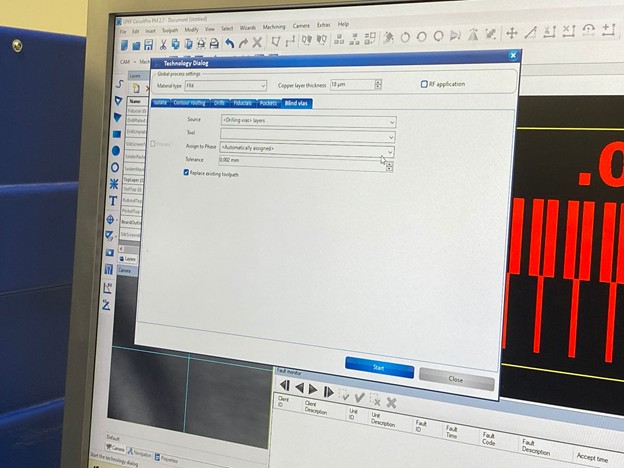
Blind Vias
Drilling creates PCB holes and vias.
Configuration includes:
- Drill layer source
- Selected drill bit
- Tolerance: 0.002 mm
This step allows the software to determine which vias to drill and which tool to use.
After done setting up those, Press Start to move on the next step, which will introduce the Tool Magazine.
8. Tool Magazine
The tool magazine displays:
- installed tools
- holder positions, from 1 - 10.
- tool life level (how worn it is). The worn level increases as the % increases.
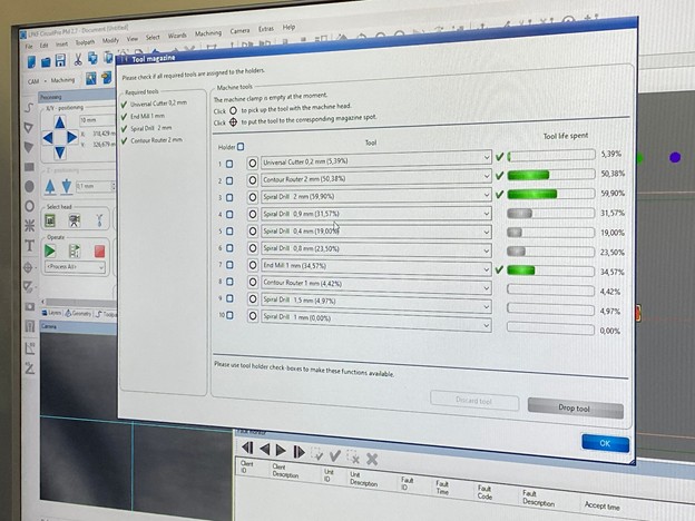
Example wear levels
| Wear | Condition |
|---|---|
| 5% | almost new |
| 50% | half life |
| 60% | worn |
9. Preparing the PCB Material
Attach FR4 board using adhesive tape, turn on the Dust Extraction unit then follow these steps:
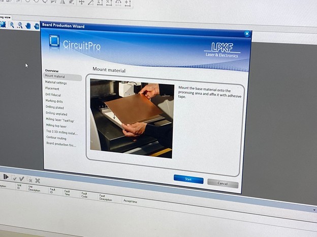
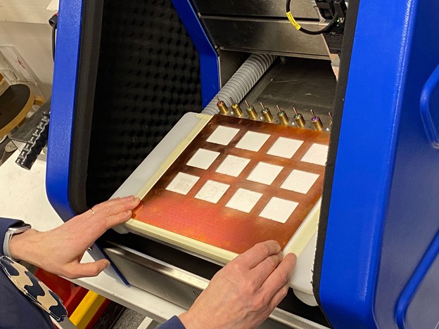
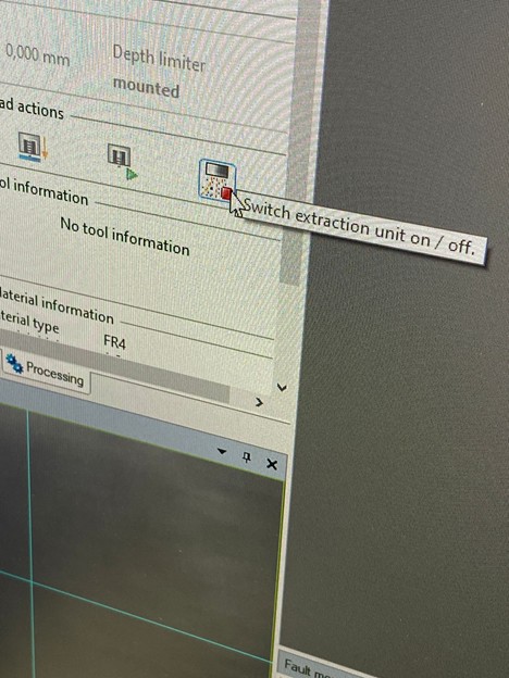
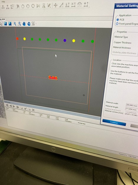
Set material position
Set the PCB material position and dimensions (material settings) in CircuitPro PM software to determine the board's location on the FR4 board before machining.
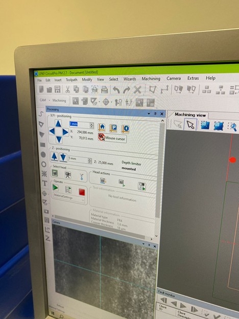
Move cutter using X‑Y‑Z control
Display the X-Y-Z axis positioning control panel of the PCB milling machine to move the cutter head and set the origin position before machining the PCB.
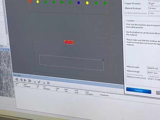
Set PCB origin
The “Placement” window is displayed in the CircuitPro PM software to position the PCB on the material sheet.
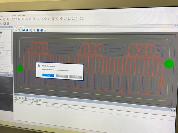
Confirm placement
A window will pop up to ask you if you want to save changes, click yes so it will have backup in case something goes wrong.
10. Milling Process
The machine will start to mill the top layer of the PCB. Set the PCB placement on the material sheet.
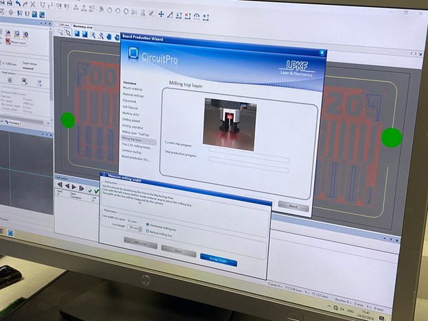
Warming up the motors
But before doing the milling process, the machine needs time to warm up the spindle motor before beginning PCB milling, takes about 2 minutes.
11. Design Rules
Before we go to our final result, let's characterize the design rules:
it is essentially about finding the "sweet spot" where your machine settings meet the physical limits of your tooling and copper board.
1. Tooling Specifications
Universal Cutter: (0.2mm) Conical Tools.
End Mill: (1mm) Flat End Mill.
Spiral Drill: (2mm) Drilling Tools.
Contour Router: (2mm).
2. Characterization Test (The Line Test)
To document our design rules, we ran the standard Linetest. This is from our STEP 9. CONFIRM PLACEMENT, where you measure lines to measure increasing width and gaps of increasing size.
3. Determining the Resolution
Analyze the test board under a microscope or a digital ome.
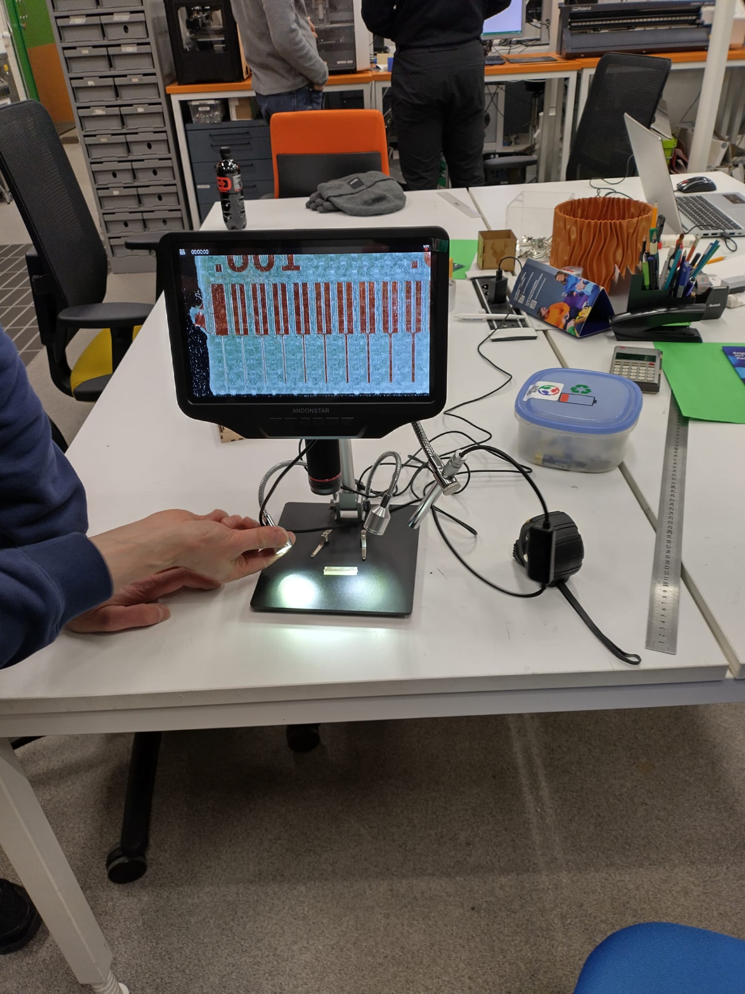
Digital microscope.
Trace Width: The traces peel off around 0.005" or 0.1mm.
Clearance: The smallest gap the 1/64" bit could actually pass through is 0.001"
4. Recommended settings for FR4/FR5
| Parameter | Trace Milling (1/64") | Outline (1/32") |
|---|---|---|
| Spindle speed | 12k--17k RPM | 12k--15k RPM |
| Feed rate | 1.5--2.5 mm/s | 2--3 mm/s |
| Plunge rate | 0.5--1 mm/s | 1 mm/s |
| Cut depth | 0.05--0.08 mm | 0.4 mm/pass |
| Total depth | 0.1 mm | 1.7 mm |
12. Finishing the Product
Cleaning up
In these two last images, we connected the suction hose and began cleaning the table by vacuuming the dust from the tabletop.
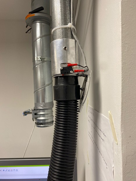
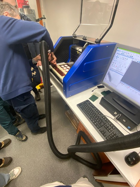
Final Product
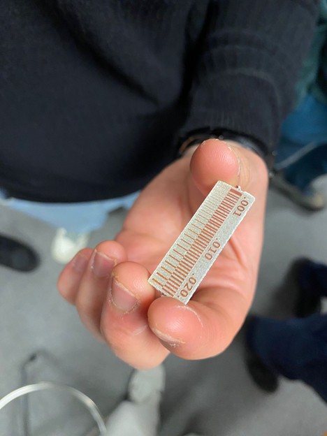
13. PCB To Boardhouse
Online PCB fabrication services
PCBs can be purchased either with parts mounted or as a board with copper tracks. Well known suppliers include PCBWay and JLCPCB. The purchasing process begins with a price quote (note: on JLCPCB an account is required to go through the entire process):
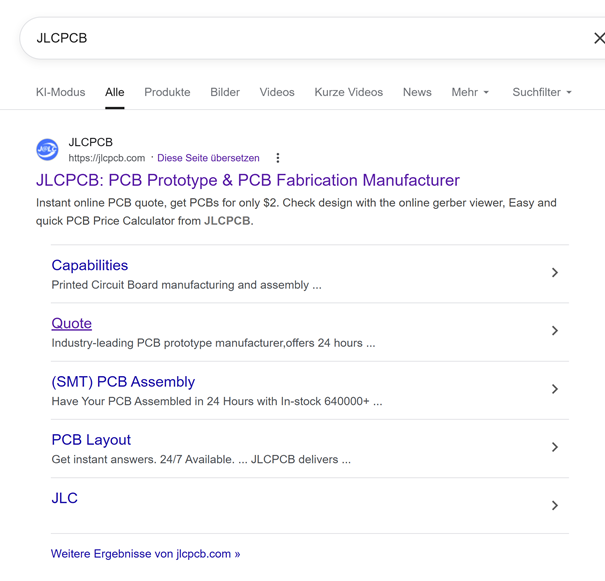
Steps to order a PCB online
In the first step of the process (on JLCPCB, although the process is almost identical across platforms), specifications of the PCBs properties as well as the gerber file are required. The gerber file can be generated as follows:
- Clicking on "file" (datei, note: German user interface)
- Selecting "plot" (plotten)
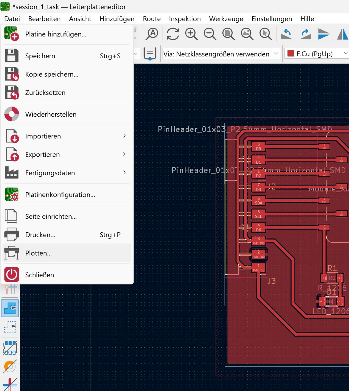
- Selecting the required settings in the pop-up window
- Plotting is completed by clicking "plot" (plotten) in the pop-up window (see notes on relevant settings below)
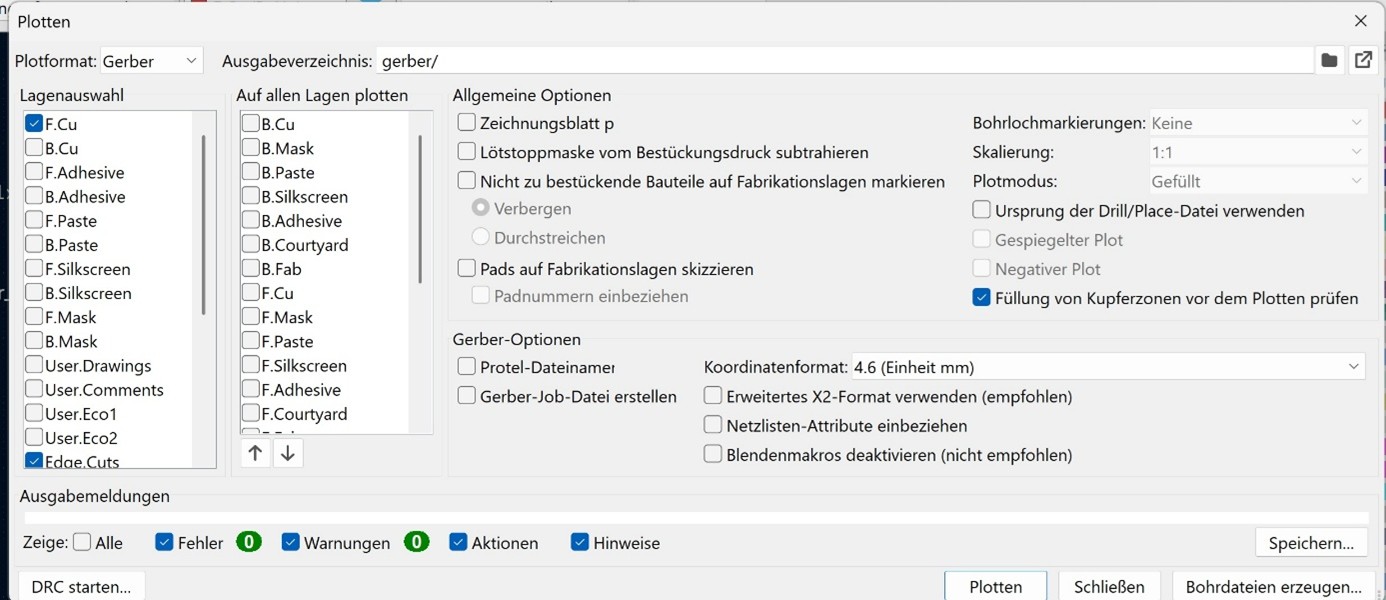
- Before in the "plot" (plotten) pop-up the required layers must be selected. A gerber file is generated for each selected layer/stage in the process. The files must be placed in a folder which must be turned into a .zip file (“send to” or “compression” ZIP-file; note here German interface).
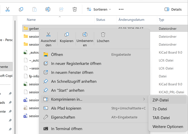

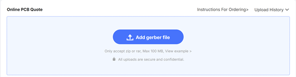
After generating the gerber.zip (note: the name “gerber” was chosen for the folder. It can be called anything), a product type must be selected on JLCPCB and the gerber.zip must be uploaded (note: PCBA is Printed Circuit Board Assembly):

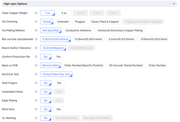
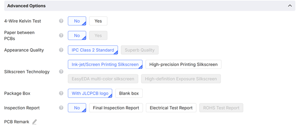
After the JLCPCB website has processed the gerber.zip, additional information regarding the PCB must be added:
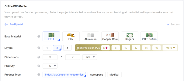
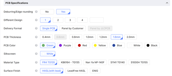
PCB assembly
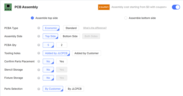
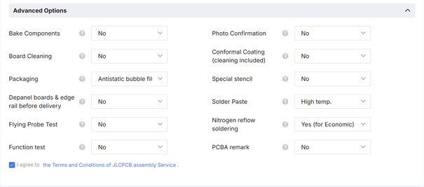
If PCB assembly is desired, this must be selected and the required information must be added:
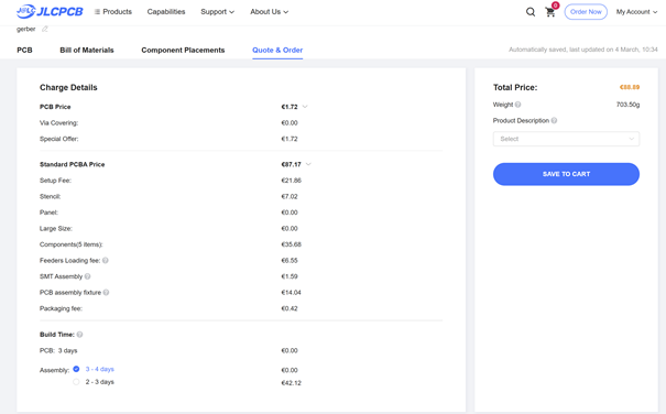
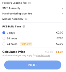
The price for the selected settings is displayed on the right throughout the process:

Click on “next” underneath the price quote:
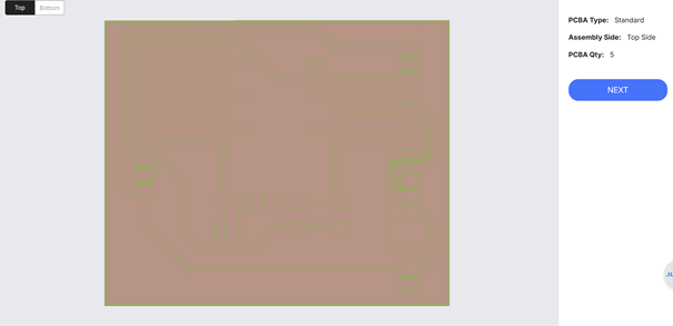
This directs the user to a PCB viewer:
After clicking on next, the user must upload a bill of materials file (BOM) and a pick and place file (CLP):
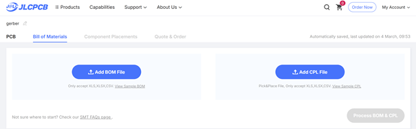
BOM and CLP files
The easiest way to generate BOM and CLP is to install the JLCPCB fabrication tool kit (other manufacturers have similar plug-ins for various software):
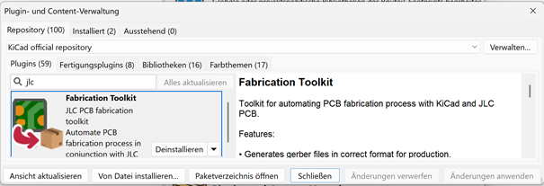
After installation, the PCB can be opened in the editor and the fabrication toolkit icon can be used to generate the required files:
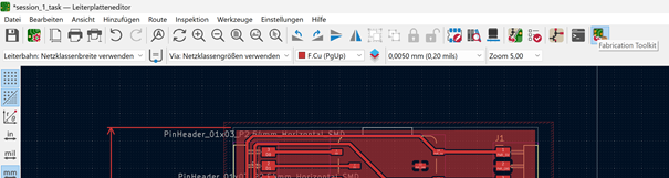
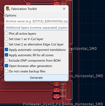
The files will be generated in the project directory in a folder named “production” by default.
Uploading files to JLCPCB
The BOM file to be uploaded is named bom.csv whilst the CLP file is named positions.csv. After uploading the files to JLCPCB, components that were not automatically matched must be selected:
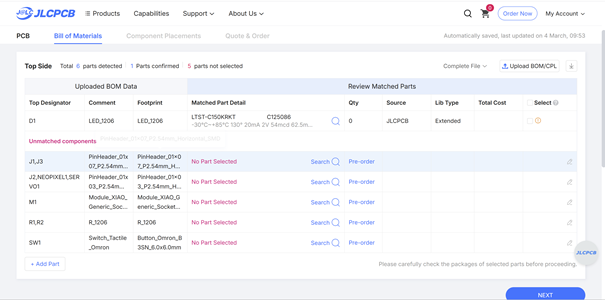
After selecting suitable components, the user can proceed to the next stage:
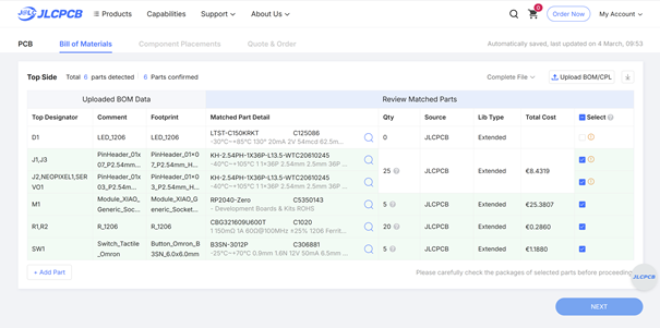
A 3D viewer allows the user to inspect the PCB before proceeding:
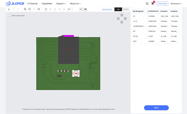
A price quote is offered and the order can proceed. The price quote will be confirmed by JLCPCB employees, as the one given at the end of the process is automated and preliminary: